Tekwizz colleagues gave me feedback on Orone-mini, my current attempt to improve Maple-mini. They suggested that the board should focus more on being practical for people, especially relatively inexperienced makers, to assemble by hand, and less on being small. We agreed this mainly means using larger SMD parts which are easier to handle. Hence, I have made the components even larger than Orone-mini, which itself already uses much larger components than Maple-mini.
Another change to help make the board easier to assemble is using bigger pads and wider tracks. This is not about making a ‘DIY’ Printed Circuit Board (PCB), but about soldering parts onto it. I’ve recently worked with a lot of people who are beginners to soldering, and they have started with through hole parts. They are making a quite finely detailed board (not designed by me:-). This experience proved it is easy to overheat pads and tracks with a soldering iron, melting the glue, and detaching the copper from the board. This can be very awkward to fix or workaround. So the Orone-mini board has wider pads and tracks around through-hole soldered parts, increasing the area of copper, and hopefully making it more robust for people to assemble.
Increasing the size of parts means increasing from the Maple-mini’s 0402, and Orone-mini’s 0805, to 1206 size Surface Mount Devices (SMD). This means all of the Maple-mini 0402 size parts, that is 0.04 inch x 0.02 inch, or approximately 1mm x 0.5mm, are now 1206 size parts, which are 0.12″ x 0.06″, or approximately 3mm x 1.5mm. So each part increase to nine times the area of the Maple-mini part. I also increased the size of the protection diodes to twice their previous size. The transistor, regulators and Integrated Circuits (ICs) are the same as before. The transistor and small regulator are about the same size as a 1206 part, and there is no other package for either IC. The through hole parts are unchanged in size; I’ve used some of them with beginners, and they seem to be okay.
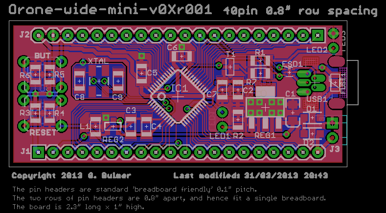
Not too surprisingly, I couldn’t fit the bigger-size components onto a Maple-mini size PCB. So the PCB has increased in size by 0.2 inches in each direction. The 0.1 inch pitch header pins are also 0.2 inches further apart, so now at 0.8 inches. It is still quite small at 2.3 inches x 1 inch. I am currently calling this ‘Orone-wide-mini’, though I quite like ‘Orone-mini-w’, or ‘Orone-mini-08’ (to identify the header spacing). Any suggestions?
Increasing the board size creates quite a lot of unused area on the bottom of the PCB, which is really the ‘Top’, because it’s the side people will see when using it. This bigger area gives more space for the ‘Top’ silkscreen, so that is slightly bigger. However, it also provided enough space to fix two other Maple-mini deficiencies; Orone-wide-mini has a ‘Power On’ LED, and a two-pin Molex socket for ‘External Power’.
The ‘External Power’ 2-pin Molex socket is on the same 0.1 inch grid as the boards main pin headers. So hopefully anyone intending to use Orone-wide-mini on their own strip-board circuits should find it practical to use 0.1 inch pin headers in the External Power holes and provide their own external power.
Finally, the component-side silk screen, which carries the names of components, has been increased in size, hopefully making it easier to use while assembling the board, and reducing the need for a separate assembly guide ‘component map’.
The header pins are as before; signal identical, and voltage identical with Maple-mini. So the existing Maple-mini-bootloader should ‘Just Work’ (TM 🙂
Here is a draft version of the ‘Orone-wide-mini’ board (or as pdf with comments Orone-wide-mini-v0Xr001):
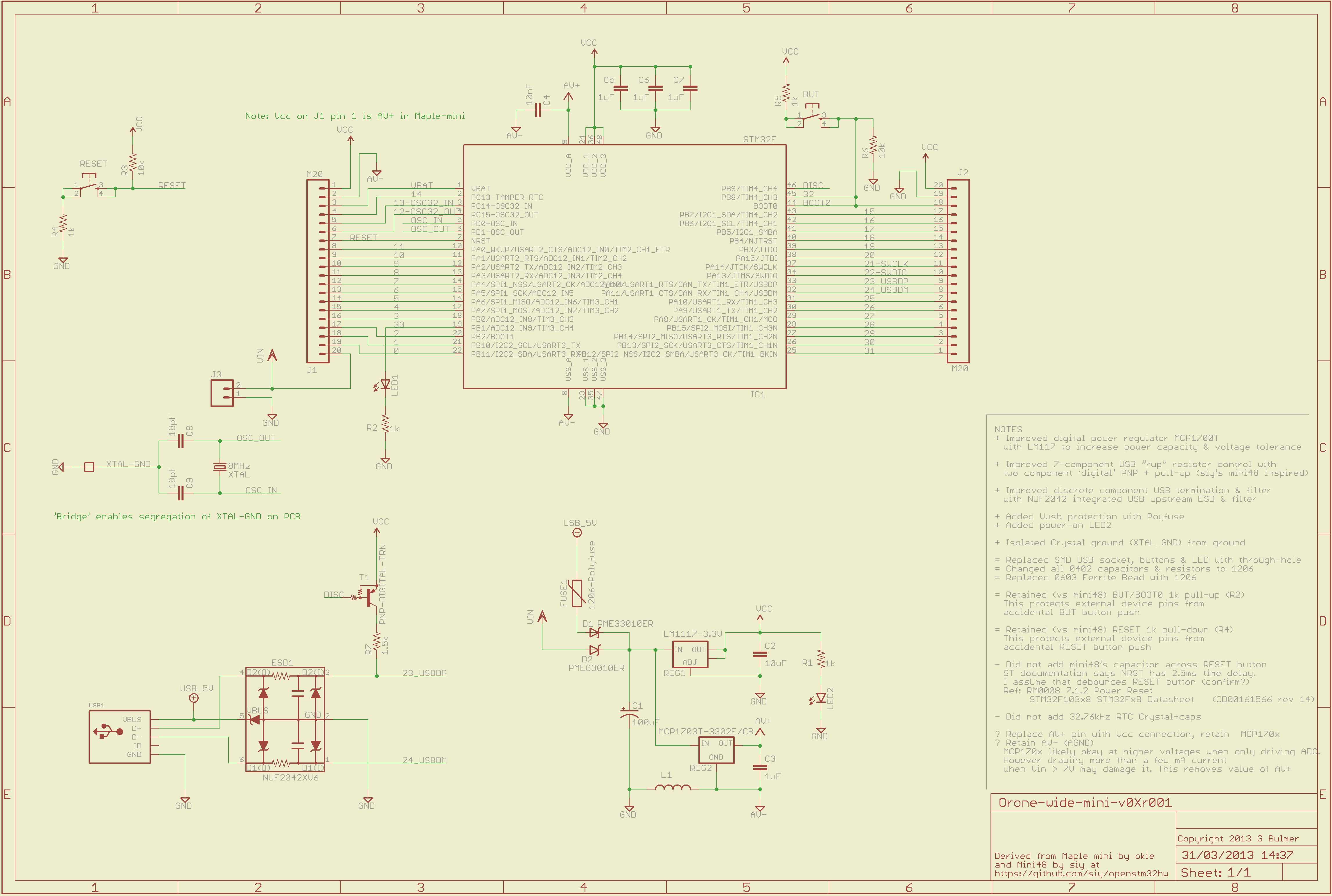
Here is the schematic with the new additions of Power-on LED and External Power Molex socket. (or as pdf Orone-wide-mini-v0Xr001.sch):
This rework has set me back a bit, and I have been ‘under the waether’, so I now hope to have checked and uploaded the CAD in a couple of days.
Summary: Orone-wide-mini uses larger components, along with bigger tracks and pads and better compnent-side silk screen to help make it ‘hand assembly friendly’. It adds a Power-on LED, an External Power 2-pin Molex socket, and larger ‘user side’ silk screen, hopefully making it more useable. It retains Maple-mini signal and voltage compatible pin headers.
WARNING: This has not yet been made, so please do not assume it even works.

March 31, 2013 at 5:42 pm |
I have a minor suggestion regarding the nomenclature you’re using to describe this board: On the board art, I see “0.8 pitch.” My understanding of pitch is that it describes the distance between *adjacent* holes or leads, rather than the spacing between the two separate SIP headers. So I suggest that you describe the connectors as 0.1″ (or 2.54 mm) pitch, and J1/J2 spacing of 0.8 inches. I suspect this documentation change may attract more novice users.
March 31, 2013 at 9:05 pm |
ursine1 – Thanks again for your helpful comments. I agree, I was sloppy using ‘pitch’ in that way. I’ve changed the pictures and pdf’s in both posts. It now reads ‘0.8″ row spacing’, which is more accurate and less confusing than row pitch. I’ve also added an explanation, visible in the .png of the header pin pitch, row spacing, and board size. Thank you.