Archive for the ‘Hands On’ Category

Improving Maple Mini (part 1)

March 26, 2013

This is a quick post to show my progress on making an improved STM32F board inspired by LeafLabs Maple-mini, and Siy’s mini48. I’ll explain more about the changes and rationale in a future post. WARNING: this board has not been assembled and tested. So please don’t assume it’s finished and ready to be used.

The main aim was to be bootloader and code compatible with Maple-mini. I believe that’s satisfied by retaining the same signal pins, for the same purposes. All the signals on the pins are the same signal sources with the same names and positions.

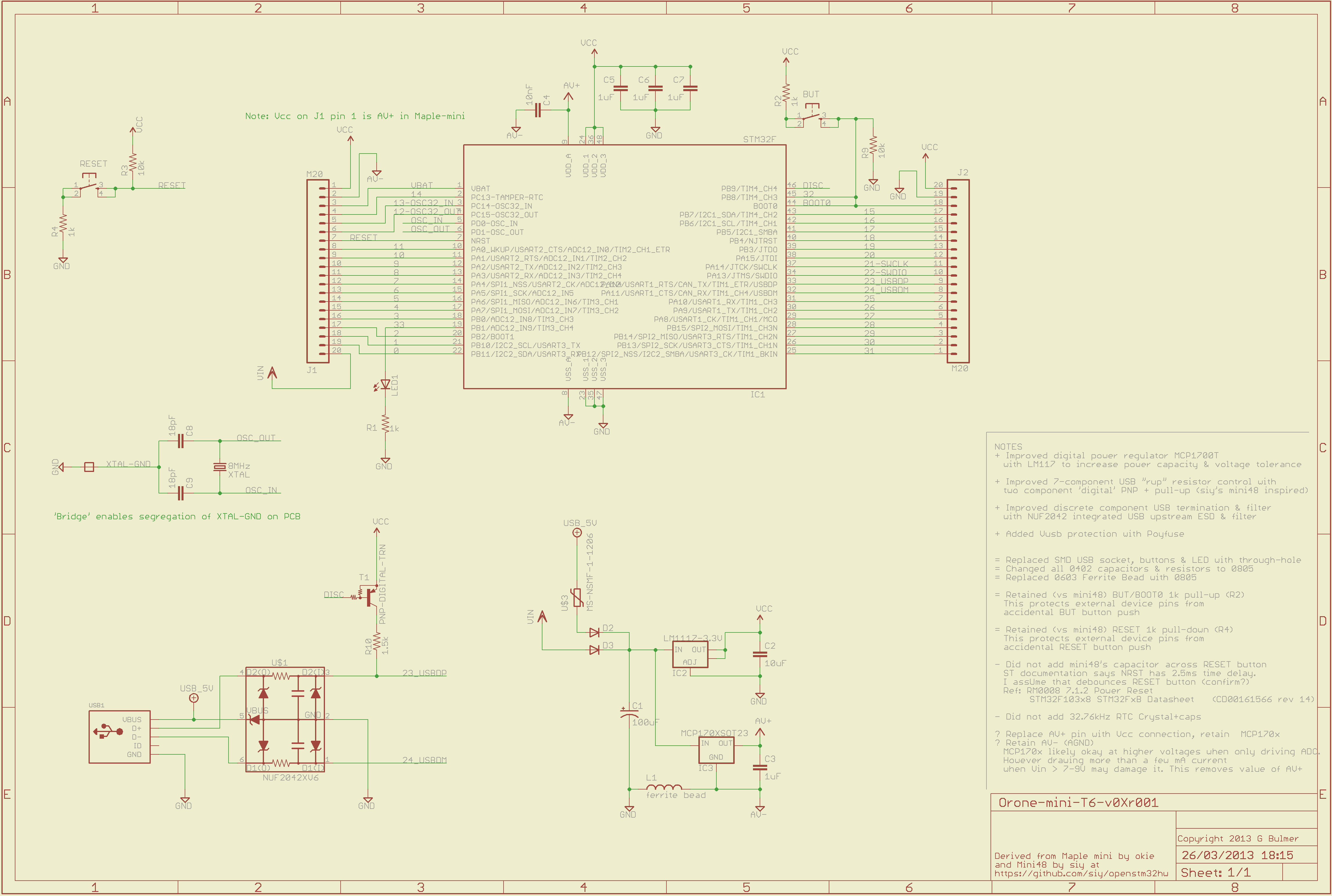
One aim was to retain pin compatibility with Maple-mini. However, as I made changes, I decided that the one of the defects of Maple-mini is the power supply. So Maple-mini’s analogue output voltage (the av+ pin) has been replaced by a connection to the higher-capacity digital power regulator. I’ll explain the detail later, but the key point is, for most uses of Maple-mini the pin-change is transparent. So I hope it is close-enough to pin compatible.

The main differences are:

  • Redesign Maple-mini’s 4-layer PCB, as simpler, Double-sided PCB
  • Single-sided Surface Mount Devices (SMD), for simpler DIY assembly
  • Larger 0805 parts, replacing 0402 parts, easier (for me) to make
  • Much higher capacity Voltage regulator, aim is full power from 9V input
  • Polyfuse protecting Host’s USB-sockets power
  • USB Electro-Static Discharge (ESD) protection for Host-USB socket
  • More compact USB termination
  • Simplified USB ‘pull-up resistor’; signals ‘USB device type change’
  • Through-hole USB socket intended to be more robust than SMD socket

When I started, I didn’t expect to achieve Maple-mini’s useful 0.6″ row spacing of header pins. I was using relatively modest PCB Design Rules of 8mil track and space (about 0.2mm track & space).

Siy wrote that he’d packed an 48 pin STM32F into a 0.5″ pitch board! He is amazingly good at this stuff.  Inspired by Siy, I tried using a finer 6mil track and cleaeence (just over 0.15mm).

Here’s the PCB. The header pins are the same pitch and distance apart as Maple-mini (or as a PDF: Orone-mini-T6-v0Xr001):

Orone-mini-T6-v0Xr001

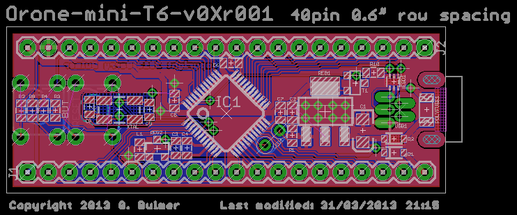
Because the header pins are physically identical, and signal identical, it should ‘just plug in’ to a circuit using Maple-mini. The only change on the header pins is replacing ‘av+’ with the normal 3.3V ‘vcc’. As I wrote, I made this change to enable the board to safely run at higher input voltages (Vin) than Maple-mini. However, I would expect the change to be invisible for most users.

There are quite a lot of changes to the schematic. So here is the schematic, including some notes about changes (or as a PDF Orone-mini-T6-v0Xr001.sch):

Orone-mini-T6-v0Xr001.sch

I intend to post more explanation, and upload the Eagle CAD to github, soon. I hope this is useful to folks.

Arduino in Schools at DD&T Conference

September 20, 2011

I had the great pleasure of leading two Arduino workshops for the DD&T Conference, on 12 July at Sheffield Hallam University.

I lead two sessions where I spoke about the background of Arduino, and the importance of Open Source. Then everyone got their “hands dirty” wiring up simple electronics and programming the Arduino. The attendees were D&T teachers, D&T support centre consultants and technicians.

Traditionally, schools use some version of the PIC microcontroller, but, I am told, schools teachers are being asked about Arduino. This is an intriguing development. It is good that there are folks out there encouraging education to get involved with Arduino, which has a very different image to the PIC-based systems.

As well as traditional breadboard-based electronics, we also tried Paul Gardiners ‘Explorer” modules. I have designed a simple Arduino shield which plugs into the Arduino, and enabled people to very quickly construct electronic systems using Paul’s electronics modules. Paul has developed almost 50 modules, so there is a lot of scope, and they can be combined to explore and develop an idea quite quickly.

The effect is transformative. Using Paul’s modules, the activity uses most of the time for programming and debugging the code. When I use breadboard-based electronics, I usually find a lot of the time is spent debugging the elctronics.

The sessions were welcomed, and worked quite well, though they were too short to cover as much ground as I would like. We have a solution to this though, because I am doing another workshop for teachers at the weekend.

Printing Wax onto PCB – Simple, Quick DIY PCB’s

January 11, 2011

I stumbled across this YouTube video at dorkbotpdx.org.

The video is presented by Jeffrey Gough of  Warranty Void If Removed. He is working to make DIY Printed Circuit Boards (PCB’s) much quicker and easier. He is aiming to reduce the PCB manufacturing process to two steps: print, etch. His ink-jet-based printing mechanism will directly print wax onto the PCB material to resist chemical etching.

The video talks about many different methods of making DIY PCB’s (maybe the first 30 minutes). Most ‘normal’ methods use printed circuit board material which is fibreglass boards covered in copper. A circuit is formed by removing the unwanted copper using a chemical etching process. The mass-production methods use photographic technology to apply an image differentiating the circuit and unwanted copper  using a technology which protects the required copper from the etching chemicals (it is actually many steps, as the industrial process is more complex than the one used by DIY PCB techniques). DIY PCB makers often use a photographic process which leaves a protective chemical ‘film’ over the required copper. This requires several steps before getting to a stage where the copper clad fibreglass can be etched into a PCB.

The approach proposed on the video is very different. Jeffrey Gough prints wax straight onto the board, and the wax resists the etching process. So there is no need to make intermediate ‘tools’ to create the photographic image, and no need for intermediate ‘manufacturing’ processes.

His approach is to modifying a low-cost (€40) Epson ink jet printer so that it can print wax straight onto blank PCB material. He did a lot of reverse engineering to build a piece of electronics which could take over driving Epson’s print head. It appears to be able to print tracks as fine as 0.1mm, which is better than most commercial PCB manufacturing process (that I can afford 🙂

The print head is heavily modified to keep the wax liquid while being printed. When liquid wax is ‘fired’ from the print head nozzle, in the same way as ink is ejected, it solidifies (freezes) on contact with the PCB copper, forming a wax covering which protects the copper from the etching chemicals.

The development is far from complete, but it shows real promise. It might revolutionise PCB production for professional design engineers, and not just DIY makers. If it were robust enough, every school and colleague that does any electronics would use it. For me, making one-off, prototype PCB’s is the slowest, and often most costly part of exploring an idea. This would remove that obstacle. By using Surface Mount Technology and Devices (SMT/SMD), I could make a PCB in well under an hour using this process. I’d use surface mount technology to minimise the drudgery of drilling hoes in the PCB. I’d solder the whole board in my trusty mini-oven using solder paste.

One slightly frustrating part is Epson could probably bring this to a production prototype stage in a few months with a few people.  If anyone at Epson is reading this, there may be a real market for such a printer, and Epson are one of the few printer manufacturers who use piezoelectric print heads, so the market may have very little competition while the products are developed, sold and improved.